NEW YORK, April 14, 2021 /PRNewswire/ --

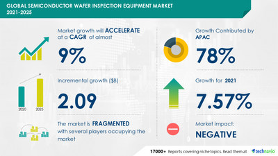
The semiconductor wafer inspection equipment market is set to grow by USD 2.09 billion, progressing at a CAGR of almost 9% during 2021-2025. The report offers an up-to-date analysis regarding the current market scenario, the latest trends and drivers, and the overall market environment.
The market is fragmented, and the degree of fragmentation will accelerate during the forecast period. Applied Materials Inc., ASML Holding NV, Camtek Ltd., Carl Zeiss AG, Hitachi High Technologies Corp., KLA Corp., Lasertec Corp., Nikon Corp., Onto Innovation Inc., and Toray Industries Inc. are some of the major market participants. The growing demand for IoT devices will offer immense growth opportunities. To leverage the current opportunities, market vendors must strengthen their foothold in the fast-growing segments, while maintaining their positions in the slow-growing segments.
Semiconductor Wafer Inspection Equipment Market 2021-2025: Segmentation
Semiconductor Wafer Inspection Equipment Market is segmented as below:
- Technology
- Optical Wafer Inspection
- Electron Beam Wafer Inspection
- End-user
- Foundries
- IDMs
- Geography
- APAC
- North America
- Europe
- South America
- MEA
To learn more about the global trends impacting the future of market research, download a free sample:
https://www.technavio.com/talk-to-us?report=IRTNTR41488
Semiconductor Wafer Inspection Equipment Market 2021-2025: Vendor Analysis and Scope
To help businesses improve their market position, the semiconductor wafer inspection equipment market provides a detailed analysis of around 25 vendors operating in the market. Some of these vendors include Applied Materials Inc., ASML Holding NV, Camtek Ltd., Carl Zeiss AG, Hitachi High Technologies Corp., KLA Corp., Lasertec Corp., Nikon Corp., Onto Innovation Inc., and Toray Industries Inc.
The report also covers the following areas:
- Semiconductor Wafer Inspection Equipment Market size
- Semiconductor Wafer Inspection Equipment Market trends
- Semiconductor Wafer Inspection Equipment Market industry analysis
Growing demand for IoT devices is likely to emerge as one of the primary drivers of the market. However, the cyclic nature of the semiconductor industry may threaten the growth of the market.
Backed with competitive intelligence and benchmarking, our research reports on the semiconductor wafer inspection equipment market are designed to provide entry support, customer profile & M&As as well as go-to-market strategy support.
Related Reports on Information Technology Include:
Global Die Bonder Equipment Market- The die bonder equipment market is segmented by end-user (OSATs and IDMs) and geography (APAC, North America, Europe, South America, and MEA). Download FREE Sample Report
Global Low-Voltage MOSFET Market- The low-voltage MOSFET market is segmented by type (41-150 V MOSFET and 0-40 V MOSFET) and geography (APAC, North America, Europe, South America, and MEA). Download FREE Sample Report
Semiconductor Wafer Inspection Equipment Market 2021-2025: Key Highlights
- CAGR of the market during the forecast period 2021-2025
- Detailed information on factors that will assist semiconductor wafer inspection equipment market growth during the next five years
- Estimation of the semiconductor wafer inspection equipment market size and its contribution to the parent market
- Predictions on upcoming trends and changes in consumer behavior
- The growth of the semiconductor wafer inspection equipment market
- Analysis of the market's competitive landscape and detailed information on vendors
- Comprehensive details of factors that will challenge the growth of semiconductor wafer inspection equipment market vendors
Table of Contents:
Executive Summary
Market Landscape
- Market ecosystem
- Value chain analysis
Market Sizing
- Market definition
- Market segment analysis
- Market size 2020
- Market outlook: Forecast for 2020 - 2025
Five Forces Analysis
- Five Forces Summary
- Bargaining power of buyers
- Bargaining power of suppliers
- Threat of new entrants
- Threat of substitutes
- Threat of rivalry
- Market condition
Market Segmentation by Technology
- Market segments
- Comparison by Technology
- Optical wafer inspection - Market size and forecast 2020-2025
- Electron beam wafer inspection - Market size and forecast 2020-2025
- Market opportunity by Technology
Market Segmentation by End-user
- Market segments
- Comparison by End-user
- Foundries - Market size and forecast 2020-2025
- IDMs - Market size and forecast 2020-2025
- Market opportunity by End-user
Customer landscape
Geographic Landscape
- Geographic segmentation
- Geographic comparison
- APAC - Market size and forecast 2020-2025
- North America - Market size and forecast 2020-2025
- Europe - Market size and forecast 2020-2025
- South America - Market size and forecast 2020-2025
- MEA - Market size and forecast 2020-2025
- Key leading countries
- Market opportunity by geography
- Market drivers
- Market challenges
- Market trends
Vendor Landscape
- Overview
- Vendor landscape
- Landscape disruption
Vendor Analysis
- Vendors covered
- Market positioning of vendors
- Applied Materials Inc.
- ASML Holding NV
- Camtek Ltd.
- Carl Zeiss AG
- Hitachi High Technologies Corp.
- KLA Corp.
- Lasertec Corp.
- Nikon Corp.
- Onto Innovation Inc.
- Toray Industries Inc.
Appendix
- Scope of the report
- Currency conversion rates for US$
- Research methodology
- List of abbreviations
Technavio's in-depth market research reports now include a thorough analysis of the COVID-19 impact on various markets to help industry leaders navigate their business through the new normal.
Download FREE Sample Report
About Us
Technavio is a leading global technology research and advisory company. Their research and analysis focus on emerging market trends and provides actionable insights to help businesses identify market opportunities and develop effective strategies to optimize their market positions. With over 500 specialized analysts, Technavio's report library consists of more than 17,000 reports and counting, covering 800 technologies, spanning across 50 countries. Their client base consists of enterprises of all sizes, including more than 100 Fortune 500 companies. This growing client base relies on Technavio's comprehensive coverage, extensive research, and actionable market insights to identify opportunities in existing and potential markets and assess their competitive positions within changing market scenarios.
Contact
Technavio Research
Jesse Maida
Media & Marketing Executive
US: +1 844 364 1100
UK: +44 203 893 3200
Email: media@technavio.com
Website: www.technavio.com/
Report Page: https://www.technavio.com/report/semiconductor-wafer-inspection-equipment-market-industry-analysis


SOURCE Technavio
© 2024 Benzinga.com. Benzinga does not provide investment advice. All rights reserved.
Trade confidently with insights and alerts from analyst ratings, free reports and breaking news that affects the stocks you care about.