Achieves Damage-Free Atomic-Level Etching with a Wide Range of Optional Functions
Hitachi High-Technologies Corporation (TSE: 8036) (Hitachi High-Tech) announced the development of the Enhanced Microwave ECR*1 Etching Module (the "Module"), a new product designed for next-generation semiconductor device manufacturing processes. The module mounts onto the 9000-Series Conductor Etch System, one of Hitachi High-Tech's conductor etch platforms and supports the development and mass production of cutting-edge semiconductor devices at 7 nm and beyond.
This press release features multimedia. View the full release here: https://www.businesswire.com/news/home/20180322005040/en/

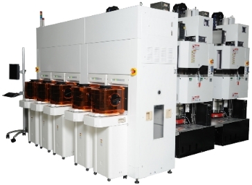
Conductor Etch System 9000-Series (Photo: Business Wire)
In the past few years, semiconductor devices evolved toward higher performance, driven by changes in transistor structures, such as FinFET*2, the commercialization of new memory techniques such as 3D-NAND, and the growing complexity of etching processes such as multi-patterning*3 technology. This evolution is accompanied by an increase in the number of etching application processes. In this environment, there has been a need for a high-performance system capable of etching at the atomic and molecular levels to support semiconductor devices in the 7 nm generation and beyond.
Hitachi High-Tech's Conductor Etch System generates a stable plasma*4 in the high-vacuum, low-pressure regime and uses the microwave ECR method capable of performing low-damage etching. The newly designed Module is an etch chamber based on a new structure that dramatically improves the exhaust capacity for reaction byproducts*5 that inhibit etching. Moreover, by optimizing the position of the magnetic-field coil, Hitachi High-Tech achieves high-precision etching that selectively controls only the thin film to be etched at the atomic and molecular levels from among the multiple thin films on which patterns will be formed, all in conjunction with maintaining low-damage etching capability.
Optional functionality of the Module includes:
|
・an Integrated Pulse Control Function*6: |
Controlling the generation of plasma and the replacement of gas within the etch chamber, thereby further enhancing etching precision. |
||
|
|
|
||
|
・Plasma Distribution Control Function: |
This function improves the magnetic coil configuration and enables more accurate control of the position where the etching plasma is generated using microwave electric field control technology, which optimizes the propagation of microwaves in the etch chamber. The combined effects enhance etching precision across the entire wafer. | ||
|
|
|
||
|
・The Multi-Temperature Control Function: |
A function designed to control the temperature of the stage on which the wafer rests by separating the stage into several zones. This allows for a uniform etching speed, which varies with temperature, across the entire wafer. | ||
Hitachi High-Tech delivers high-precision etching capabilities through the wide range of functions available with this Module. By doing so, Hitachi High-Tech will continue to provide innovative solutions in a timely manner to address a diverse array of customer needs for the development and mass production of semiconductor devices. In parallel, Hitachi High-Tech contributes to cutting-edge manufacturing by pursuing and creating new value together with its customers.
| *1 |
ECR(Electron Cyclotron Resonance: Applying a magnetic field to a vacuum system starts a rotational motion of electrons called cyclotron motion centered at the magnetic field lines in the magnetic field. When microwave energy with frequency (ω) matching the rotation speed is made incident, energy resonance occurs between the cyclotron motion and the electric field, and the electric field energy is absorbed by the electrons. This is called electron cyclotron resonance. It effectively accelerates electrons and can apply a large amount of energy. The plasma that is generated with the energy applied in this way is called ECR plasma. |
|
| *2 |
FinFET(Fin-shaped Field Effect Transistor: A field effect transistor with a 3D-type construction |
|
| *3 |
Multi-patterning: A technique for forming fine circuit patterns through repeated, multiple exposures |
|
| *4 | Plasma: A group of charged particles that is kept almost electrically neutral as a whole. The ions with a positive charge and electrons with a negative charge are distributed equally in an ionized state. | |
| *5 | Reaction byproducts: By-products generated by chemical reactions between reaction gases used in etching and the materials being etched. | |
| *6 | Integrated Pulse Control Function: A function that controls the timing of factors such as the generation of plasma, the replacement of reaction gases, and the detachment and emission of reaction products. | |

View source version on businesswire.com: https://www.businesswire.com/news/home/20180322005040/en/
© 2024 Benzinga.com. Benzinga does not provide investment advice. All rights reserved.
Trade confidently with insights and alerts from analyst ratings, free reports and breaking news that affects the stocks you care about.